Converting an electron image into a digital image
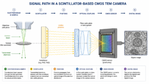
In Transmission Electron Microscopy (TEM), the sample is illuminated by a high-energy electron beam. As the electrons pass through sample, they are scattered, diffracted (according to the structure and composition of the sample) and the resulting electron distribution will be converted into a visible image can be displayed. One of the common approaches is indirect electron detection using a scintillator. In this architecture, the electrons first interact with a scintillator, where their energy is converted into visible photons. The resulting light image is then transferred to a digital image sensor, typically a CMOS sensor.
The basic signal chain is:
This seemingly simple conversion process involves several carefully matched components. The performance of the complete camera depends not only on the CMOS sensor, but on the scintillator, optical coupling, pixel size, electronics and image-processing software working together.
The role of the scintillator
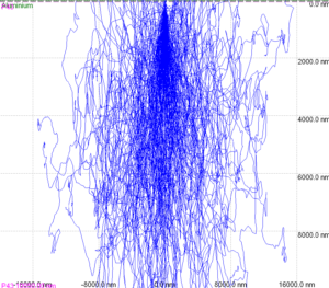
Electron Scattering in the Scintillator
The scintillator is the first detector element encountered after the electron beam has passed through the sample. When the electrons enter the scintillating material, part of their energy is converted into visible light. The spatial distribution of this light corresponds to the electron microscope’s image. Therefore the scintillator’s light output, spatial resolution, thickness and interaction with the optical coupling system all contribute to the overall detector performance. For example the scintillator thickness should be adjusted to the TEM electron beam energy (eg 120kV vs 200kV) and adjusted to the coupling technique and sensor’s pixel size.
Thus simply selecting a high-resolution CMOS sensor does not automatically produce a high-performance TEM camera. The detector must be considered as a complete electron-to-photon-to-digital imaging system.
From photons to CMOS
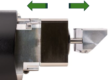
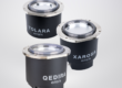
The photons generated by the scintillator are transferred to the camera sensor through an optical coupling system. Different camera designs use different approaches, including fibre-optic coupling and lens-based optical coupling. In a fibre-coupled design, an optical fibre transfers the scintillator image to the sensor. A tapered fibre can also change the image scale, allowing the scintillator area and sensor pixel size to be matched more effectively. This tapered principle is used in EMSIS bottom-mounted cameras, like the XAROSA and QEDIRA which allows the effective pixel size and field of view to be optimized together.
Resolution, sensitivity and noise: finding the balance
The conversion from electrons to photons and then from photons to electronic signal inevitably introduces additional factors that influence detector performance. Important parameters include:
- Spatial resolution – how accurately fine structures are reproduced.
- Conversion Efficiency – how efficiently the detector converts the available electron signal into useful image information.
- Signal-to-noise ratio – particularly important when working with weak signals or low-dose imaging.
- Dynamic range – the ability to record weak and strong intensities simultaneously.
- Frame rate – important for specimen navigation, in-situ experiments and dynamic processes.
- Field of view – particularly important for overview imaging and specimen searching.
- Scintillator and optical coupling efficiency – determining how effectively the electron-generated light reaches the sensor.
Research on scintillator-based TEM detectors has shown that the detector point-spread function and noise characteristics are important components of overall image quality.
A complete detection system, not simply a camera sensor
The main conclusion is that a TEM camera should be regarded as a complete detection system. The electron beam carries the information, the scintillator converts that information into light, the optical coupling transfers and potentially scales the image, the CMOS sensor converts the photons into electronic data, and the acquisition software turns those data into a usable scientific image.
The performance of a modern TEM camera is ultimately determined by how well these individual elements are matched. This is where detector engineering—scintillator selection, optical coupling, sensor technology, electronics and software—becomes just as important as the megapixel count of the camera.
EMSIS ASIA
TEM CAMERAS

X
- No products in the list