Why Tapered Fibre Coupling
In Transmission Electron Microscopy (TEM), the quality of the final image depends not only on the CMOS sensor itself, but on how efficiently the electron image is transferred from the scintillator to the sensor. For bottom-mounted TEM cameras, tapered fibre-optic coupling provides an efficient and highly stable solution for matching these two components. In comparison to conventional 1:1 fibre-optic coupling or a lens-based optical coupling system, a tapered fibre optic deliberately changes the image scale between the scintillator and the camera sensor. This makes it possible to optimise the relationship between scintillator resolution, photon collection, sensor pixel size and field of view.
How does a tapered fibre optic work?
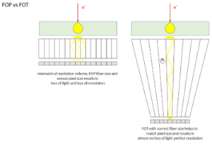
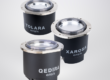
In a TEM camera, the incoming electrons first interact with a scintillator, where they are converted into visible light, which is transferred to the camera sensor. With a conventional 1:1 fibre-optic coupling, the image is transferred at approximately the same scale from the scintillator to the sensor. A tapered fibre optic, in contrast, has a larger input surface and a smaller output surface. The image is consequently demagnified as it travels through the fibre taper. This allows a relatively large scintillator area to be coupled efficiently to a smaller CMOS sensor. The result is an increased effective pixel size at the scintillator and, importantly, a larger usable field of view without requiring an excessively large sensor. EMSIS uses carefully selected tapered fibre optics in its bottom-mounted cameras, QEDIRA, XAROSA and TOLARA, in which the tapered fibre is specifically designed to match the CMOS pixel size and scintillator, providing a large field of view while maintaining high sensitivity.
The importance of matching the scintillator and sensor
The scintillator determines how incoming electrons are converted into photons and therefore plays a major role in the achievable resolution and sensitivity of the camera. Modern CMOS sensors can have very small physical pixels. Simply placing such a sensor behind a scintillator does not necessarily provide the best TEM image. If the sensor pixels are significantly smaller than the useful resolution delivered by the scintillator, the system may effectively oversample the optical image without gaining corresponding spatial information.
A carefully designed fibre taper addresses this, by demagnifying the scintillator image, several sensor pixels can effectively correspond to a larger area of the scintillator. This increases the amount of signal represented by each effective camera pixel and can provide an excellent balance between resolution, sensitivity and field of view. The EMSIS bottom-mounted cameras optimize this “perfect match” between pixel size, fibre optics and scintillator.
Tapered fibre versus 1:1 fibre coupling
A 1:1 fibre-optic plate offers a straightforward and efficient way of transferring the scintillator image to the sensor. However, the image scale cannot be optimised independently of the physical sensor dimensions.
A tapered fibre provides an additional degree of freedom: magnification can be designed into the fibre-optic coupling itself.
This can provide several advantages:
- Larger effective pixel size at the scintillator
- Improved matching between scintillator resolution and sensor pixel size
- Larger field of view for a given sensor format
- High photon-transfer efficiency without introducing a conventional lens system
- Compact and mechanically stable construction
- Excellent suitability for both high-resolution imaging and diffraction applications
The practical benefit is particularly relevant as CMOS sensors continue to offer higher pixel counts and smaller physical pixels. Rather than simply increasing the number of pixels, the complete detector chain can be optimised around the characteristics of the TEM scintillator.
Optimised detector performance
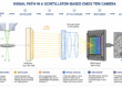
The key advantage of tapered fibre technology is therefore not simply higher resolution. It is the ability to optimise the complete electron-to-digital image chain. The electron beam is converted into photons by the scintillator; the tapered fibre transfers and scales this optical image; and the CMOS sensor converts it into a digital image. When these three components are carefully matched, the camera can achieve an effective combination of sensitivity, spatial resolution, field of view and speed.
The EMSIS bottom-mounted cameras – QEDIRA, XAROSA, TOLARA – demonstrate this principle carefully matched fibre optics, scintillator and pixel size.
EMSIS ASIA
TEM CAMERAS

X
- No products in the list