-


A correctly calibrated TEM is of highest importance for generating correct imaging data. Using the MAG*I*CAL calibration standard, three TEM calibrations can be performed:
- Magnification over the entire range from 1000x up to 1,000,000x magnification
- Camera constant calibration using the Si single crystal (for indexing diffraction patterns)
- Image/Diffraction pattern rotation using the same Si single crystal
The MAG*I*CAL traceable TEM calibration standard consists of 4 sets of 5 SiGe layers with a thickness of ~10nm, alternating with pure silicon layers with a thickness of ~13nm. The total thickness of the set of alternating layers is ~100nm. The distance between each set of 5 layers is ~1.2µm. The epitaxial layers are grown using an MBE (Molecular Beam Epitaxy) process on a single crystal silicon {001} substrate. The finished calibration standard is a cross-sectioned TEM calibration sample with four regions where the calibration lines can be imaged
The four sets of alternating layers of Si and SiGe provide light and dark lines with good contrast. These four sets of the alternating layers are calibrated using a high resolution transmission electron microscope (HR-TEM) with reference to the {111} lattice space of silicon (0.3135428nm) measured on the single crystal substrate of the MAG*I*CAL calibration standard. This method provides unbroken traceability of the natural fundamental constant; the lattice constant of silicon (see image below left). All calibration markings on the standard are directly referenced to this natural constant. The calibrated values can be verified by the user by observing the crystal lattice image of the silicon substrate and validating the calibrated values.
-

EM-Tec FS22 combines two F12 FIB grid holders with two standard 12.7mm (1/1) pin stubs within a 27x27mm footprint. Both the F12 FIB grid holders and the pin stubs can be rotated independently in the holder for selecting the optimum orientation in the FIB/SEM system. The EM-Tec FS22 dual FIB grid and sample holder enables loading the samples and FIB grids close together. The FIB grid and the sample stubs are at the same level when using Si wafer samples.
-

EM-Tec FS21 combines the EM-Tec F12 FIB grid holder with two standard 12.7mm (1/2) pin stubs. The F12 FIB grid holder and the sample stubs can be rotated in the holder for selecting the optimum orientation in the FIB/SEM system. The EM-Tec FS21 FIB grid and sample holder enables loading the samples and FIB grids close together. The FIB grid and the sample stubs are at the same level when using Si wafer samples
-

EM-Tec FS22 combines two F12 FIB grid holders with two standard 12.7mm (1/1) pin stubs within a 27x27mm footprint. Both the F12 FIB grid holders and the pin stubs can be rotated independently in the holder for selecting the optimum orientation in the FIB/SEM system. The EM-Tec FS22 dual FIB grid and sample holder enables loading the samples and FIB grids close together. The FIB grid and the sample stubs are at the same level when using Si wafer samples
-

EM-Tec FS21 combines the EM-Tec F12 FIB grid holder with two standard 12.7mm (1/2) pin stubs. The F12 FIB grid holder and the sample stubs can be rotated in the holder for selecting the optimum orientation in the FIB/SEM system. The EM-Tec FS21 FIB grid and sample holder enables loading the samples and FIB grids close together. The FIB grid and the sample stubs are at the same level when using Si wafer samples
-

The finely dispersed thin gold particles on a carbon film provide an excellent high resolution TEM standard. The gold particle size distribution is normally in the 2nm to 9nm range. Image quality, magnification and instrument stability are readily determined. For resolution assessment, this standard offers a choice of crystalline orientation on static or low tilt stages. The thickness of the crystals can be calculated form the projected shape of the gold crystal. The background noise from the structure of the carbon support film helps in determining the operating transfer function.
-

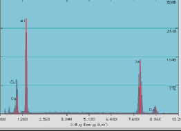
A thin copper foil on an aluminium TEM grid provides well defined and separated lines of Al (K-line) and Cu (K- and L-lines) in an EDX spectrum. These lines can be used to calibrate the EDX spectrometer and to asses EDX detector efficiency. The carbon coated 60nm Cu foil is mounted on a 200 mesh aluminium TEM grid.
-

Oriented gold crystal provides plane spacing of 0.102, 0.143 and 0.204nm. Used for checking resolution, image quality, magnification and instrument stability in high resolution TEMs. The single oriented gold crystals produces a characteristic diffraction patterns. When the TEM is correctly setup, it should resolve the 0.102 nm (100 plane) planar spacing, 0.143 nm (220 plane) and the 0.204nm (200 plane). Since these are physical constants they can also be used for magnification calibration. Mounted on a 400 mesh Au TEM grid.
-

The combined test specimen standard provides a 3 in 1 method for testing the performance of the TEM. The combined test specimen consists of graphitised carbon particles on a holey carbon which are shadowed with gold. Combines astigmatism test using perforated carbon film with resolution tests using graphitised carbon black and fine gold particles. The evaporated gold forms small polycrystalline islands in which lattice fringes can be resolved. The combined test specimen can also be used for contamination measurements by noting the carbon depositing rate within the holes of the gold film. Mounted on a 300 mesh copper TEM grid
-

This TEM test standard provides Platinum/Iridium particles evaporated on a holey carbon film. The holes in the carbon film are useful for focussing and astigmatism corrections. The small crystals of Pt/Ir provide excellent high contrast particles for resolution checks using the point separation test. Provided on a 300 mesh Cu TEM grid.


